How to Avoid EMC Failures by Following Proper Design Practices
Designers have to take many engineering options into consideration when designing a product. From component choices to casing decisions, the design and construction of a product takes considerable time and effort. Of particular concern to the designer, however, is how well their product will fare in the final testing stage.
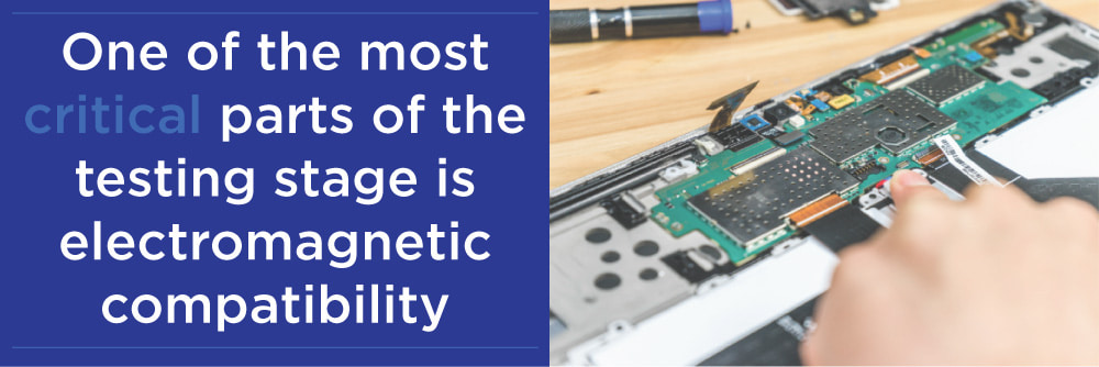
One of the most critical parts of the testing stage is electromagnetic compatibility (EMC). EMC tests essentially measure two things in a product — its ability to operate as intended within its intended environment (immunity testing) and also a device’s potential to cause harmful interference to other devices operating in its vicinity (emissions testing).
Immunity testing gauges how a device reacts when exposed to various forms of electromagnetic disturbances or phenomena, while emissions testing measures the amount of electromagnetic energy (conducted and radiated) the device generates.
Both are extremely important aspects which the designer must consider during the design stage. If not controlled properly, the resulting electromagnetic incompatibility can negatively affect the surrounding environment, contributing to product failures, safety protocol breaches, data losses and more.
Why Designs May Fail EMC Testing
Averting a failed EMC compliance test simply involves using basic design rules during the design and manufacturing processes. To avoid costly EMC testing failures, we have listed some of the most common reasons designs fail EMC testing, why these failures occur and how to avoid them through proper design practices:
1. Avoid Interrupting the Signal Return Plane
Placing a split, gap or cut in the signal return or ground plane is rarely necessary for any board under normal circumstances. Adding these interruptions can result in more problems than solutions. Most predominant of these problems is the increased time and effort needed to design ways to control the flow of low-frequency currents.
If you are absolutely convinced your board truly needs a split, gap or cut in the signal return plane to prevent low-frequency coupling problems, seek additional help or advice. An expert can check your work, make suggestions and help you come up with solutions to help you execute the gap effectively. It’s important to remember that what worked for another design may not work the same way in yours.
2. Don’t Place High-Speed Circuitry Between Connectors
Too many designers overlook this simple rule. Bypassing this detail can result in bloated designs, requiring shielding and filtering than should be necessary.

The placement of connectors on the printed circuit board (PCB) is crucial because the cabling attached to these connectors act as very effective antennas, especially at frequencies below two to three hundred MHz. While PCB traces can also act as antennas, their effects tend to be electrically small in relation to the wavelength at these frequencies. This makes PCB traces relatively inefficient radiators. Cable lengths are typically much closer to the optimum wavelengths at these frequencies, making them much more efficient radiators.
Usually, this isn’t a problem — when these connectors are arranged along a single edge of a board, the voltage between them is relatively small. However, when high-speed circuitry is located between the connectors, higher potential differences can develop, causing RF currents on the cable’s shield and/or conductors. This in turn causes the cable to radiate, potentially resulting in the product exceeding emissions requirements.
3. Ensure Auxiliary Equipment Is Compliant
During emissions testing, manufacturers are required to connect auxiliary equipment to all I/O ports using commercially available cables. This ensures the usage of all ports within the device, demonstrating the device’s full functionality. This typically presents a worst-case scenario, causing the device to produce maximum emission levels.
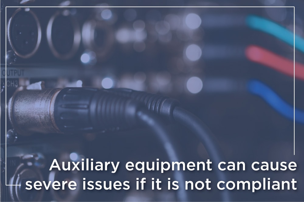
This step is extremely important to the testing process, and yet improper auxiliary equipment can cause severe issues. As an example, if you use a non-compliant device, such as a low-quality USB flash drive, the emissions test can produce skewed readings. This is not because of your device — it is because of the non-compliant auxiliary equipment. The readings caused by this non-compliant equipment can send you and your production team into an unnecessary investigation into emissions issues that simply aren’t there. Not only can this severely delay your product’s release, but it can also cost your company thousands in man-hours and re-booking fees for the test lab.
4. Find Proper LCD Displays
An LCD display can affect a product’s radiated emissions performance as much as any other part. This is primarily because not all LCDs are made the same way. Even if they look the same, one LCD may emit much more noise than one from another manufacturer due to differences in design.
Handling this problem depends largely on the LCD display used within the product. In most cases, testing multiple screens at a time from multiple manufacturers by ordering samples is a pragmatic way to go. This way, the tester can pre-scan each display to determine which would be the best to minimize emissions.

On the other hand, this practice is much less feasible with larger, more expensive LCD displays. It is even less doable with custom LCD displays, as multiple custom orders may need to be put in.
The best way to avoid this problem is to order from a trusted manufacturer that can back up their emissions ratings. Additionally, mitigating the emissions by designing around the screens can produce positive results. For example, if the LCD connects to the rest of the device with a flex cable or DIP connector, adding a signal filter to your design could be just as effective.
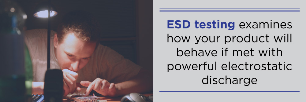
5. Prepare for ESD Testing
Electrostatic discharge testing, also known as ESD testing, is an important requirement for general CE testing. This testing process examines how your product will behave if met with powerful electrostatic discharge. The process usually involves the application of two to eight-kV ESD pulses applied to the exposed metallic surfaces of the product (contact discharge) and also to insulated surfaces (air discharge). ESD testing can cause serious damage to the product.
To improve a product’s performance and avoid damage from ESD testing, the designer can take the following few measures:
- Pinpoint ESD testing locations. These are areas of the device that can be touched without using special equipment or dismantling the product. Exploratory testing on the casing is one part of this process, where the tester touches all exterior portions of the product’s chassis. If the chassis is non-conductive, other common testing points include the connectors, screw heads, keypads and buttons, chassis seams, displays and areas where internal PCBs and components come close to the chassis.
- Identify ESD testing levels. Typically, discharges are applied at incrementally increasing voltage levels, from two kilovolts to four kilovolts for contact discharge and from two kilovolts to eight kilovolts for air discharge. These levels can vary based upon your product and intended installation environment. Consult with your test laboratory or refer to the applicable standards for your product to determine the exact test levels to be applied for your product.
- Choose an appropriate suppressor. Find ESD protection for your circuit board. Keep in mind that this protection must be appropriate for the test levels to be applied to your product. Spark gaps, resistors, capacitors, varistors and TVS diodes are all good suppressors for this purpose, but they must fit appropriately within your product without causing problems of their own.
- Apply suppressors to the proper locations. Once you have the protective components, be sure to place them as close to the problem area as possible. This minimizes the series inductance caused by any routing between the discharge location and the suppressor.
- Think about the discharge path. Closely consider the discharge path for applied ESD. In many designs, the chassis ground is separated from the main board ground for safety reasons. A common method is to bring your chassis ground on your circuit board ground back to the main power input. This allows any discharges to dissipate without affecting the rest of the circuitry.
6. Manage Signal Transition Times
Well-formed digital signals at lower harmonic frequencies are considerably greater in amplitude than the higher harmonics. Slowing the transition times of digital signals can further reduce these higher harmonics. However, increasing the transition time too much can begin to degrade the signal integrity. Finding the ‘sweet spot’ is key.

Three common methods for controlling rise and fall times include:
- Control the slew-rate with a logic family. This is often the most effective option for applications, especially with a matched termination.
- Placing a resistor or ferrite in series with the device’s output. Controlling the rise time of a circuit gives a designer more control while typically costing less than the other options listed. Ferrite is similarly effective but costlier.
- Put a capacitor in parallel with the device’s output. Capacitors can increase the amount of high-frequency current pulled by the source device. This is usually the least useful choice for transition time control, but it works under some circumstances.
7. Minimize Loop Areas
One of the simplest, most common mistakes made in circuit board designs is the addition of loop areas associated with high-frequency currents. This is often a result of designer oversight, especially if the designer doesn’t know where the currents flow.

To avoid this problem, circuit designers should be aware of the following:
- Signal currents always return to their source. Because of this, current paths are always loops.
- Signal currents take the path of least impedance. For high-frequency currents, this tends to be the path of least inductance. For lower frequency currents, this is the path of least resistance.
8. Reduce RF Noise on Cables
Cables tend to emit RF noise easily, which can increase a product’s emissions overall and cause the product to fail radiated emissions tests.
If your completed design seems to have issues with radiated emissions, the first thing you should do to try to find the problem is to detach as many cables as possible. If the emission disappears, you’ll know that the noise was radiating from one of the detached cables. Use a simple process of elimination by reconnecting the cables one by one until the problem emission reappears. In some cases, multiple cables may be the source of the issue, making it harder to identify and handle the problem cables.

While one should keep these steps in mind to mitigate these issues after they happen, it is best to minimize any unintended RF energy as much as possible during the design phase. Designers accomplish this by minimizing signal slew rates, as discussed previously in item 6.
There are hundreds of ways to mitigate the effects these signals have on emissions, but they can be prevented with a few simple design practices. The first of these design practices involves adding in-line ferrite beads to your power supply and static I/O signals, or simply placing 0 Ohm resistors as placeholders in areas where ferrite beads may be needed in the future. These inline beads function as noise suppression beads, which are specifically designed to absorb RF energy and convert it into heat. The second of these suggestions involves providing adequate power supply de-coupling at connectors.
9. Select the Right Power Adapter
A noisy power supply or power converter can contribute a great deal of noise to your device, negatively affecting the device’s emissions performance during testing. For this reason, it’s important to select a power adapter appropriate for your device’s emissions class.

An emissions class is essentially a rating describing the intended use of your device. Class A devices, for example, are designed for use in business, industrial and commercial environments, while class B devices can be used in these areas as well as residential locations. Of these two classes, B requirements are much stricter than class A requirements, with much lower limits on emission levels. This difference in requirements means it’s important to understand your device’s class and find an appropriate power supply.
In addition to this requirement, you should also consider:
- Accommodating for the power adapter. Power adapters are usually tested with DC resistive loads, which are fundamentally different from dynamic loads. This means the emission characteristics of the adapter may be different when connected to a dynamic load with a broader current supply spectrum. This difference in current characteristics can potentially result in more emissions than advertised. To minimize the effects of this difference, you may need to specifically design your power circuitry to handle a broader current supply spectrum.
- Investing in better adapters. Numerous manufacturers will stretch the truth when it comes to their compliance testing. This is especially common among manufacturers of lesser quality — or less pricey — products, as it reduces their bottom line and maximizes their profits. For this reason, it doesn’t hurt to put a little bit more time and money into a quality adapter from a trusted manufacturer.
- Requesting a test report from the manufacturer. It never hurts to double-check the equipment you are purchasing, especially if it is coming from a new manufacturer. Many manufacturers will provide test reports to support their claims about their equipment.
10. Use Shielding for Over Sensitive Circuitry
EMC immunity testing can interfere with sensitive analog circuits, which is why you should protect them with a well-grounded conductive shield. The energy in an RF field can induce small currents, which can interfere with the operation of your circuits, especially sensors and other more sensitive parts.
By adding a conductive shield around any of these sensitive parts, you can avoid most of these negative effects during CE testing.
11. Find a Trusted Expert in EMC
Over half of all consumer products fail their test for EMC compliance, which is why in-house testing can be such an important part of the manufacturing process. Pre-compliance testing not only allows your company to identify compliance issues and rectify them before a formal test, but it also saves you money by eliminating the need for multiple tests, rescheduling fees and labor costs.

Are you looking to purchase equipment for pre-compliance testing? Com-Power Corporation is here to help. We are a leading manufacturer in the field of electromagnetic compatibility, and our high-quality products are designed to help you find, measure and identify sources of electromagnetic noise in your product. We work through a vast network of representatives and distributors on both local and global levels to meet the needs of customers worldwide.
We take considerable pride in our EMC test equipment, which you can use to properly test your products, both formally and informally. Our testing products feature all the accuracy and abilities needed for testing for most EMC regulatory standards. Even better, we deliver all products pre-calibrated, complete with NIST traceability and documentation. We even offer annual re-calibrations that are completed by our highly trained technicians, so your equipment continues to function at peak precision and accuracy.
Since 1989, our goal as a company has been to provide our customers with the finest products and best support in the industry. We strive to constantly improve our products and design new ones to help our customers meet their goals, because we want to see you succeed.
To learn more about the products and services we offer, please contact us today.